PCB Design Course in Coimbatore
Master Circuit Design and Simulation with Industry-Standard Tools
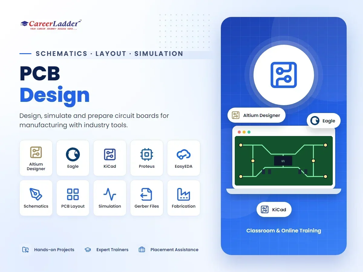
About the PCB Design Course
Master circuit design, schematic capture, and layout using industry-standard PCB tools.
Train at our Avinashi Road (Hope College, Peelamedu) or Sundarapuram branch in Coimbatore — or join online — with hands-on projects, industry mentors, and dedicated placement support from day one.
Every electronic product — from an EV charger to a smart water-level controller — begins life as a printed circuit board, and PCB designers are the engineers who turn a circuit idea into a manufacturable board. Career Ladder’s PCB Design course covers the complete flow: component selection and schematic capture, footprint and library creation, placement and routing, multilayer stack-up planning, and the design-for-manufacturing (DFM) checks that decide whether a fabrication house can actually build your board at a sane cost and yield.
Tool fluency is a core goal. You work across the EDA tools the industry actually screens for — Altium Designer for professional high-speed work, KiCad as the open-source standard, Eagle for quick commercial projects, and Proteus for simulating circuits before committing copper. Alongside tools, the course drills the engineering judgment that separates a layout operator from a designer: grounding strategy, decoupling, trace-width and clearance decisions, thermal relief, EMI awareness, and reading component datasheets for land patterns and layout notes.
Learning this in Coimbatore has a practical edge. The region — long celebrated as the Manchester of South India for its motor, pump, and textile-machinery industries — is steadily adding electronics to its products: motor controllers, VFD interfaces, battery management, sensor boards, and IoT retrofits for legacy machines. Product startups and electronics manufacturing units in Tamil Nadu need designers who can carry a board from schematic through Gerber release, and India’s national push for local electronics manufacturing keeps expanding that demand.
The course is available in classroom mode at our Hope College (Peelamedu, Avinashi Road) and Sundarapuram branches, and as live online training. Career Ladder has taught 10,000+ students and holds a 4.6-star Google rating across 1,500+ reviews. Placement assistance comes standard: portfolio and resume shaping around your fabricated boards, mock interviews with layout-review-style questions, and referrals to hiring partners in electronics design and manufacturing.
Course Syllabus
Module-by-module curriculum — expand each to see the topics covered.
Module 1:Electronics Foundations for Board Designers+
- Passive and active components: behavior, packages, and ratings
- Reading datasheets: absolute maximums, pinouts, and layout notes
- Through-hole vs SMD technology and package families (0402–TQFP–BGA)
- Power supplies, regulators, and decoupling fundamentals
- Analog vs digital signals and mixed-signal awareness
Module 2:Circuit Simulation with Proteus+
- Building and simulating circuits before layout
- Testing amplifier, timer, and microcontroller circuits virtually
- Virtual instruments: oscilloscope, meters, and signal sources
- Catching design errors early to reduce board respins
Module 3:Schematic Capture Done Right+
- Schematic hierarchy, sheets, and readable circuit organization
- Net naming, net classes, and power/ground symbols
- Design reuse and multi-channel schematics
- Electrical Rule Check (ERC) and annotation
- Generating netlists and syncing schematic to layout
Module 4:Library & Footprint Creation+
- Symbol creation standards and pin mapping
- Footprint design from datasheet land-pattern drawings
- IPC-7351 land pattern basics
- 3D models and STEP file association
- Managing personal and team component libraries
Module 5:PCB Layout Fundamentals (KiCad & Eagle)+
- Board outline, mounting holes, and mechanical constraints
- Component placement strategy: signal flow and functional grouping
- Trace width, clearance, and current-carrying calculations
- Ground planes, copper pours, and stitching vias
- Silkscreen, assembly markings, and fiducials
- Design Rule Check (DRC) discipline
Module 6:Professional Layout with Altium Designer+
- Altium environment: projects, ActiveBOM, and draftsman documents
- Rules-driven design: net classes, rooms, and constraints
- Interactive routing: push, hug, and differential pairs
- Polygon management and layer stack configuration
- Variants, outputs jobs, and release packaging
Module 7:Multilayer & High-Speed Design Concepts+
- Two-layer vs four-layer-plus stack-up decisions
- Impedance control and controlled-length routing basics
- Crosstalk, return paths, and EMI/EMC-aware layout
- Via types: through, blind, buried, and microvia awareness
- Layout for switching regulators and noisy power sections
- ESD protection and connector-area layout practices
Module 8:Design for Manufacturing, Assembly & Test+
- DFM rules: annular rings, solder mask dams, and acid traps
- Panelization, tooling strips, and fabrication tolerances
- DFA: component spacing, orientation, and wave vs reflow constraints
- Testpoints and design-for-test basics
- Talking to fab houses: quoting, capabilities, and feedback loops
Module 9:Outputs, Fabrication & Bring-Up+
- Gerber and drill file generation and verification
- BOM preparation and pick-and-place (centroid) files
- Ordering prototypes from Indian and global fab services
- Hand-soldering SMD and through-hole assembly practice
- Board bring-up, testing, and debugging first prototypes
- Capstone board review and portfolio presentation
Who Should Join This Course
Real-World Projects You Will Build
- 1IoT sensor node board: design a compact two-layer board with an ESP32 module, sensor interfaces, USB programming circuit, and battery management — from schematic to ordered prototype.
- 2Motor-driver board: layout for a DC motor-control board with proper separation of power and logic sections, wide current-carrying traces, and thermal copper planning relevant to motor-and-pump-country applications.
- 3SMPS/power-supply board: a buck-converter layout exercise focused on tight switching loops, feedback-node care, and input/output filtering.
- 4Four-layer microcontroller mainboard in Altium: stack-up definition, ground-plane strategy, decoupling networks, and rules-driven routing with a complete release package (Gerbers, BOM, assembly drawings).
- 5Library-building assignment: create verified symbols, IPC-compliant footprints, and 3D models for a ten-component kit purely from manufacturer datasheets.
- 6Capstone product board: your own circuit concept taken through simulation, capture, layout, DFM review, fabrication ordering, hand assembly, and live bring-up — a physical board you can put on the interview table.
Career Scope & Opportunities
PCB design opens roles such as PCB Layout Engineer, Hardware Design Engineer, E-CAD Layout Engineer in design-services firms, Component/Library Engineer, and DFM/NPI Engineer inside electronics manufacturing services (EMS) companies. Because layout sits between circuit design and production, skilled designers interact with — and often grow into — hardware architecture, signal integrity, and NPI project roles.
The demand backdrop in India is strong and structural. Government-backed electronics manufacturing incentives, EV and energy-storage growth, and the localization of products that were previously imported all require boards designed and revised in India. Tamil Nadu is one of the country’s biggest electronics manufacturing states, and Coimbatore’s own industrial base — motors, pumps, controllers, textile-machine electronics, and a rising set of IoT startups — generates steady work for designers who understand both electronics and the industrial products they go into.
Indicative compensation: junior layout engineers in India typically begin around 2.5–4.5 LPA, mid-level designers with three to five years and multilayer/Altium depth often earn roughly 6–12 LPA, and high-speed or signal-integrity specialists in product companies and semiconductor-adjacent firms can move well beyond that. As always, these are hedged market ranges — actual offers track your tool mastery, portfolio quality, and employer type.
A practical career note: PCB design rewards demonstrable work more than most fields. A candidate who walks in with two or three fabricated, working boards and can defend every placement and routing decision consistently outperforms paper-qualified applicants. The course is built to give you exactly that evidence, and Career Ladder’s placement assistance — resume building, mock design-review interviews, and hiring-partner referrals — helps convert it into offers.
What You Will Master
100% Placement Assistance
Resume building, mock interviews, and direct referrals to our hiring partners — until you land the role.
Frequently Asked Questions
Do I need an electronics background?+
Yes, a basic understanding of electronics components (Resistors, Capacitors, etc.) is helpful. We cover the design tools from scratch.
What software will I learn?+
We cover industry-standard tools like Eagle, Altium Designer, KiCad, and Proteus for simulation.
Is this course practical?+
Absolutely. You will design, print, and assemble your own PCB boards during the course.
Which EDA tool should I focus on for my first job?+
Learn concepts on KiCad or Eagle, but make sure your portfolio includes Altium Designer work — it is the most commonly listed tool in Indian hardware job postings. The course sequences tools that way deliberately, so you can adapt to whichever platform an employer uses.
Will my boards actually get fabricated during the course?+
Yes. You generate real Gerber packages, learn how prototype fabrication services work, and go through assembly and bring-up so you experience the full loop — including discovering how layout mistakes show up on physical boards, which is where the deepest learning happens.
Is PCB design at risk from AI auto-routers?+
Auto-routing has existed for decades and still cannot make the judgment calls that matter — stack-up choice, power integrity, EMI strategy, DFM trade-offs, and component sourcing realities. AI features are becoming assistants inside EDA tools; the engineer who understands why a layout works remains essential and is what companies hire for.
What is the difference between a PCB design engineer and a hardware design engineer?+
Hardware design engineers define the circuit — selecting ICs, calculating values, and owning the schematic — while PCB layout engineers turn that schematic into a manufacturable board. In smaller companies one person does both, which is why this course covers circuit understanding, simulation, and layout rather than layout alone.
Do I need to be good at soldering to succeed in this course?+
No prior soldering skill is expected. We teach enough hand-soldering for prototype assembly and bring-up, because designers who have assembled their own boards make noticeably better layout decisions — but your career value comes from design skill, not production soldering.
Our Coimbatore Branches
Hope College (Peelamedu)
1st Floor, 267, Avinashi Road, Peelamedu (Hope College), Opposite GRG Ladies Hostel, Above Sneha Hospital, Coimbatore 641004
+91 88702 75880
Sundarapuram
1st Floor, Bank of Baroda Building, 5, Madukkarai Main Rd, opp. Abirami Hospital, Sundarapuram, Coimbatore
+91 88070 28071
Related Courses
Embedded Systems & IoT
Learn the foundations of embedded systems, IoT, and hardware programming.
PLC SCADA
Master industrial automation with hands-on training in PLC programming and SCADA systems.
AutoCAD Electrical
Master electrical design and drafting with AutoCAD Electrical for industrial applications.